Unifying photoelectron spectroscopy and transport measurements: the current-induced insulator-to-metal transition in Ca2RuO4
Certain oxides can be switched from highly insulating to conducting, opening many possibilities for applications in electronics. Especially important are cases in which this switching can be achieved electrically, for instance by applying a current or a voltage. Ca2RuO4 is a material in which such switching can be realised by applying a small current. So far, however, the electronic structure of the current-induced conductive phase has been completely unknown. This is mainly due to the difficulty of performing photoelectron spectroscopy experiments from a sample when applying a current: the accompanying voltage drop across the size of the light spot is detrimental to the experimental energy resolution. In our experiment, we have solved this problem by using a very small UV light spot, such that the current-induced voltage drop is negligible. The measurements then directly reveal the electronic structure of the current-induced conductive phase. Surprisingly, it is quite similar to the equilibrium phase and it is the formation of small domains of a slightly different structure that is responsible for the increased conduction. Photoemission experiments with a small light spot can also be used to directly map the electrical potential landscape across the surface of a material and thereby provide the result of voltage / current transport measurements directly from photoemission. The figure below shows how the sample becomes increasingly conductive for higher currents (as measured by the density of states at the Fermi level) and that this process starts at the left side of the sample (the negative electrode). Also shown is the externally measured I / V curve with the typical negative differential resistance in such a phase transition. These findings greatly increase the scope of photoemission measurements, from a static technique to an approach that can access electrically-driven non-equilibrium situations and reveal both spectroscopic and transport properties.

Current driven insulator-to-metal transition without Mott breakdown in Ca2RuO4, Davide Curcio, Charlotte E. Sanders, Alla Chikina, Henriette E. Lund, Marco Bianchi, Veronica Granata, Marco Cannavacciuolo, Giuseppe Cuono, Carmine Autieri, Filomena Forte, Alfonso Romano, Mario Cuoco, Pavel Dudin, Jose Avila, Craig Polley, Thiagarajan Balasubramanian, Rosalba Fittipaldi, Antonio Vecchione and Philip Hofmann, arxiv2303.00662
Physical Review B, in press.
A surface molecular movie: Tracking the vibrational motion of surface atoms in real time
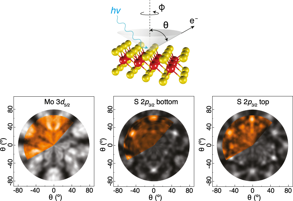
The vision of a “molecular movie” refers to our ability to track the motion of atoms and molecules on the ultimate length and time scale: we wish to see exactly how bonds between atoms change and since this can happen very fast, a time resolution on the order of 100 femtoseconds is required. In this experiment, we have been using the structural technique of X-ray photoelectron diffraction to track the vibrational motion of surface atoms after exciting such a vibration with a short laser pulse. The key difficulty in this experiment is that it needs an X-ray laser emitting short pulses. For our experiment, we have used the free electron laser FLASH in Hamburg. The time-resolved X-ray photoelectron diffraction patterns then reveal the motion of the surface atoms in detail for the first 2 picoseconds after launching the vibration. The figure below shows a sketch of the experimental setup, the interatomic distances d1 and d2 that can be tracked by the technique and the measured diffraction pattern before the system is excited. The experiment is a proof-of-principle for realising molecular movies, something that can eventually be used to track important processes such as reactions in heterogeneous catalysis.

Tracking the surface atomic motion in a coherent phonon oscillation, Davide Curcio, Klara Volckaert, Dmytro Kutnyakhov, Steinn Ymir Agustsson, Kevin Bühlmann, Federico Pressacco, Michael Heber, Siarhei Dziarzhytski, Yves Acremann, Jure Demsar, Wilfried Wurth, Charlotte E. Sanders and Philip Hofmann, arxiv2205.13212
Physical Review B 106, L201409 (2022).
Core level line shape as a thermometer for electronic temperature
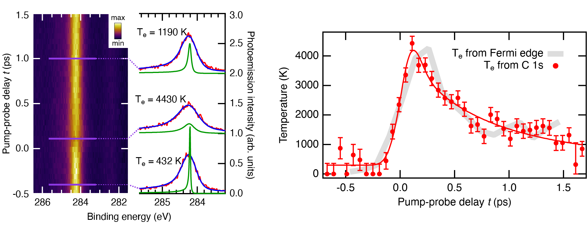
X-ray photoelectron spectroscopy (XPS) is a hugely versatile technique for chemical analysis, revealing not only the elements a sample is composed of, but also their detailed chemical environment. Since XPS is also very surface sensitive, it has been especially important to detect chemical changes during surface reactions in heterogeneous catalysis. Now ultrafast X-ray sources, such as free electron lasers, give the possibility to study chemical reactions and even electronic processes on their natural time scale of hundreds of femtoseconds or picoseconds and exploring the physics of XPS on this time scale has become an important research subject. When inspecting the XPS C 1s line shape of graphene after an ultrafast optical excitation, we have made a surprising discovery: The XPS peak undergoes a strong broadening that can be understood in terms of an increased electronic temperature (not lattice temperature) in the sample (the figure shows both the broadened spectra and the time-dependent temperature as red markers). The electronic temperature determined in this way agrees well with that determined directly from the statistical distribution of the valence band electrons (grey line). This means that the core level line shape can not only be used as a “thermometer”, it has the prospect of generally detecting transient ultrafast electronic excitations.
Ultrafast electronic line width broadening in the C 1s core level of graphene, Davide Curcio, Sahar Pakdel, Klara Volckaert, Jill A. Miwa, Søren Ulstrup, Nicola Lanata, Marco Bianchi, Dmytro Kutnyakhov, Federico Pressacco, Günter Brenner, Siarhei Dziarzhytski, Harald Redlin, Steinn Agustsson, Katerina Medjanik, Dmitry Vasilyev, Hans-Joachim Elmers, Gerd Schönhense, Christian Tusche, Ying-Jiun Chen, Florian Speck, Thomas Seyller, Kevin Bühlmann, Rafael Gort, Florian Diekmann, Kai Rossnagel, Yves Acremann, Jure Demsar, Wilfried Wurth, Daniel Lizzit, Luca Bignardi, Paolo Lacovig, Silvano Lizzit, Charlotte E. Sanders, Philip Hofmann, arxiv2105.10472
Phys. Rev. B 104, L161104 (2021).
Measuring the electronic structure of an operating transistor
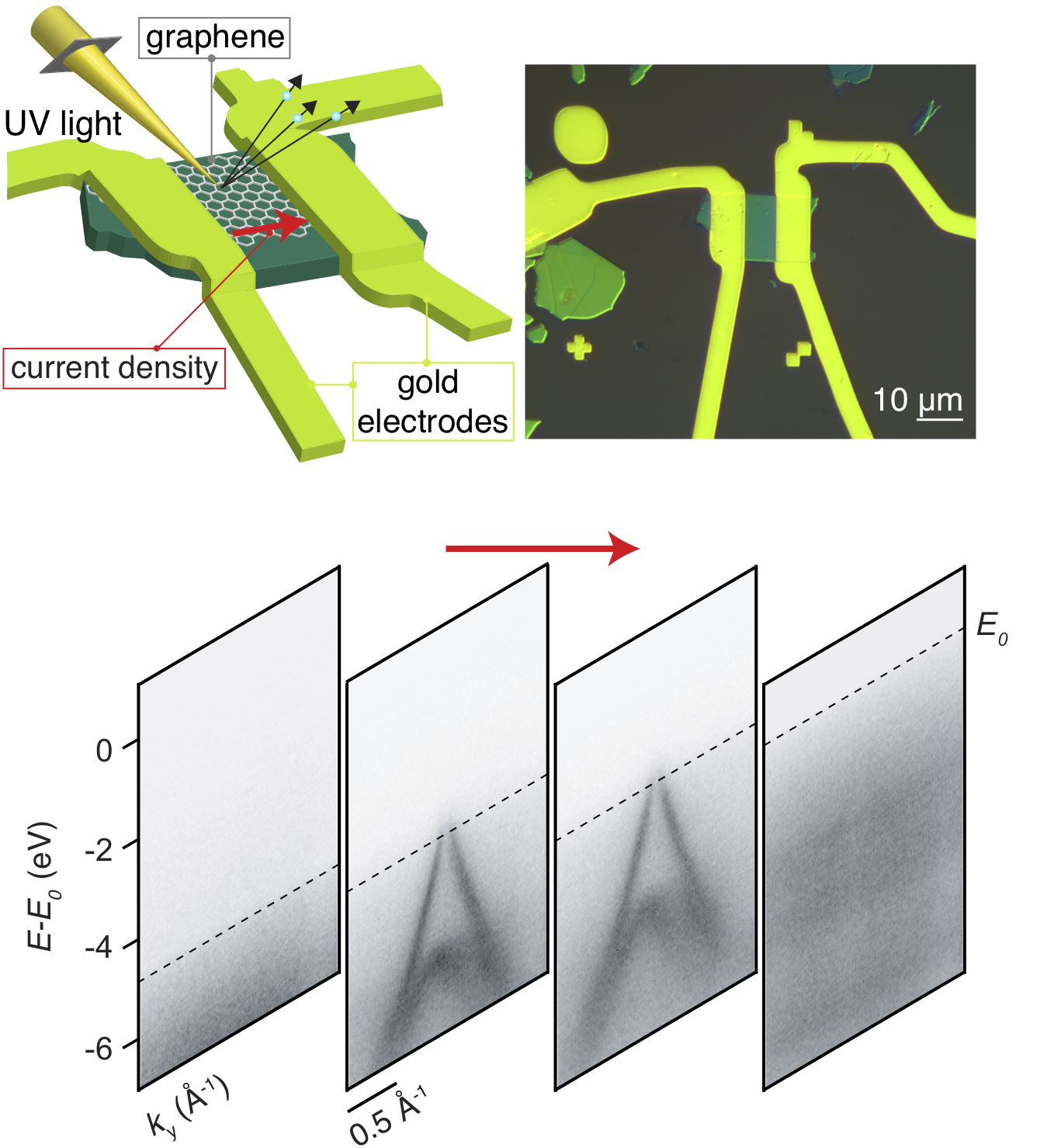
Modern electronics is based on the ability to turn currents on and off in a transistor, but it has so far been unknown if and how the presence of a current affects the property of the working material in the transistor. Using angle-resolved photoemission spectroscopy with a highly focused nano-scale light spot, we have been able to study the electronic properties of graphene in a field effect transistor geometry with and without an applied current. The figure shows a sketch of the device, a small piece of graphene contacted by two gold electrodes, together with a microscopic image. The device is quite small – only about 10 microns in length – but it is still possible to collect spectra when moving the light beam across it, as shown in the lower part of the figure. The presence of the current creates a voltage drop across the sample and the energy of graphene’s Dirac cone is thus position dependent. The combination of spectroscopic and transport measurements gives a huge amount of information on the local lifetime, carrier density and mobility. The novel approach to integrate transport with ARPES measurements will be particularly interesting for novel quantum materials in which the current density can influence the properties of the material as such, for example by triggering an insulator-to-metal transition.
Accessing the spectral function in a current-carrying device, Davide Curcio, Alfred J. H. Jones, Ryan Muzzio, Klara Volckaert, Deepnarayan Biswas, Charlotte E. Sanders, Pavel Dudin, Cephise Cacho, Simranjeet Singh, Kenji Watanabe, Takashi Taniguchi, Jill A. Miwa, Jyoti Katoch, Søren Ulstrup, Philip Hofmann, arxiv:2001.09891
Physical Review Letters, 125, 236403 (2020).
Momentum-resolved linear dichroism in bilayer MoS2
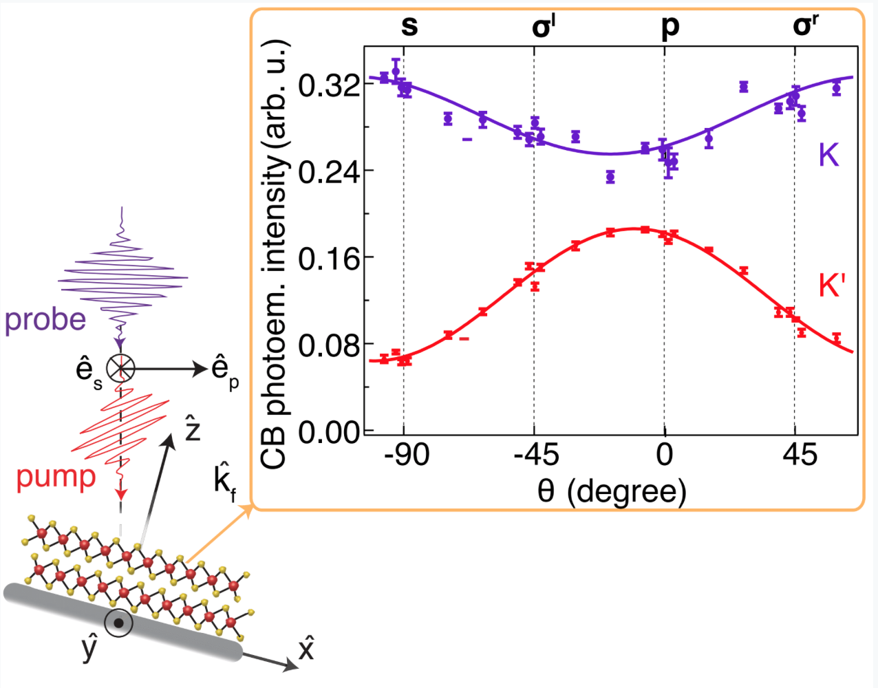
Information about the symmetry and orbital character of electronic wave functions can be determined via photoemission selection rules that shape the measured intensity in an ARPES experiment. In a time-resolved ARPES experiment, the intensity contains additional information about inter-band excitations induced by an ultrafast laser pulse with tunable polarization. We take advantage of this capability to explore the polarization-dependent photoemission intensity in the transiently-populated conduction band of bilayer MoS2. We find a strong linear dichroism effect in the conduction band of bilayer MoS2. To support our experimental findings, we provide an effective model to evaluate the one-electron dipole matrix elements governing optical excitations and the photoemission process. In the case of single-layer MoS2, we find a significant masking of intensity outside the first Brillouin zone, which originates from an in-plane interference effect between photoelectrons emitted from the Mo orbitals. For the bilayer, an additional inter-layer interference effect leads to a distinctive modulation of intensity with photon energy. We then model the polarization-dependent photoemission intensity in the transiently-populated conduction band using the semiconductor Bloch equations. Our theoretical analysis reveals a strongly anisotropic momentum-dependence of the optical excitations due to intra-layer single-particle hopping, which explains the measured linear dichroism in bilayer MoS2.
Momentum-resolved linear dichroism in bilayer MoS2, Klara Volckaert, Habib Rostami, Deepnarayan Biswas, Igor Markovic, Federico Andreatta, Charlotte E. Sanders, Paulina Majchrzak, Cephise Cacho, Richard T. Chapman, Adam Wyatt, Emma Springate, Daniel Lizzit, Luca Bignardi, Silvano Lizzit, Sanjoy K. Mahatha, Marco Bianchi, Nicola Lanata, Phil D. C. King, Jill A. Miwa, Alexander V. Balatsky, Philip Hofmann, Søren Ulstrup, arxiv1910.01848
Physical Review B, in press 100, 241406(R) (2019).
Layer and orbital interference effects in photoemission from transition metal dichalcogenides, Habib Rostami, Klara Volckaert, Nicola Lanata, Sanjoy K. Mahatha, Charlotte E. Sanders, Marco Bianchi, Daniel Lizzit, Luca Bignardi, Silvano Lizzit, Jill A. Miwa, Alexander V. Balatsky, Philip Hofmann, Søren Ulstrup, arxiv1910.01882
Physical Review B 100, 235423 (2019).
Single-layer, single-orientation transition metal dichalcogenides
Semiconducting singe-layer transition metal dichalcogenides such as single-layer MoS2 and WS2 are thought to hold huge potential in (opto) electronic applications because of the so-called valley degree of freedom and the possibility to couple this to optical excitations. The concept of “valley-tronics” derived from this could be used to store or transmit quantum information. Alas, the possibility to exploit the distinct valley polarisation in a grown sample relies on the fact that the entire sample is grown in a single orientation, without the presence of the very common so-called mirror domains. In a collaboration between scientists in Italy and Aarhus, we have realised the growth of single layer MoS2 and WS2 in a single orientation and exploited this to study resulting effects of valley- and spin-polarisation in these materials. The single orientation is demonstrated in photoelectron diffraction experiments. It can be directly seen in the diffraction patterns in the figure, as these show a three-fold rather than a six-fold symmetry.
Novel single-layer vanadium sulphide phases, Fabian Arnold, Raluca-Maria Stan, Sanjoy K. Mahatha, H. E. Lund, Davide Curcio, Maciej Dendzik, Harsh Bana, Elisabetta Travaglia, Luca Bignardi, Paolo Lacovig, Daniel Lizzit, Zheshen Li, Marco Bianchi, Jill A. Miwa, Martin Bremholm, Silvano Lizzit, Philip Hofmann, C. E. Sanders, arxiv1803.07999
2D Materials 4, 0454009 (2018).
Suppression of Mirror Domains in the Epitaxial Growth of Single Layer WS2, Luca Bignardi, Daniel Lizzit, Harsh Bana, Elisabetta Travaglia, Paolo Lacovig, Charlotte E. Sanders, Maciej Dendzik, Matteo Michiardi, Marco Bianchi, Moritz Ewert, Lars Buß, Jens Falta, Jan Ingo Flege, Alessandro Baraldi, Rosanna Larciprete, Philip Hofmann, Silvano Lizzit, arxi1806.04928, Physical Review Mat. 3, 014003 (2019).
Spin structure of K valleys in single-layer WS2 on Au(111), Philipp Eickholt, Charlotte Sanders, Maciej Dendzik, Luca Bignardi, Daniel Lizzit, Silvano Lizzit, Albert Bruix, Philip Hofmann, Markus Donath, arxiv1807.11235
Physical Review Letters 121, 136402 (2018).
Larger than 80% Valley Polarization of Free Carriers in Singly-Oriented Single Layer WS2 on Au(111), H. Beyer, G. Rohde, A. Grubišic Cabo, A. Stange, T. Jacobsen, L. Bignardi, D. Lizzit, P. Lacovig, C. E. Sanders, S. Lizzit, K. Rossnagel, P. Hofmann, M. Bauer, arxiv1907.10553, Physical Review Letters, in press.
Novel single-layer vanadium sulphide phases
Most novel two-dimensional materials studied so far are extracted from existing “parent” materials that can be viewed as stacks of van der Waals bonded layers. The two-dimensional version is then simply one isolated such layer, e.g. graphene whose parent compound is graphite. It is an intriguing question if there are any truly new materials in two dimensions that do not have a bulk analogue. In this work, we have discovered several phases of two-dimensional vanadium sulphide. Some can be though as a simple layer extracted from a bulk VS2 crystal, but one phase is entirely new and has no known bulk analogue.

Novel single-layer vanadium sulphide phases, Fabian Arnold, Raluca-Maria Stan, Sanjoy K. Mahatha, H. E. Lund, Davide Curcio, Maciej Dendzik, Harsh Bana, Elisabetta Travaglia, Luca Bignardi, Paolo Lacovig, Daniel Lizzit, Zheshen Li, Marco Bianchi, Jill A. Miwa, Martin Bremholm, Silvano Lizzit, Philip Hofmann, C. E. Sanders, arxiv1803.07999
2D Materials, 4, 0454009 (2018).
Ultrafast Band Structure Control of a Two-Dimensional Heterostructure
The band gap in a bulk semiconductor is a characteristic feature of the material and can usually not be modified without, for instance, massive chemical substitution. For a two-dimensional material this is quite different: It is well known that the band gap of two-dimensional semiconductors such as MoS2 or WS2 can be changed drastically, merely by placing these materials onto substrates with different dielectric properties. This is due to the screening properties of the substrate that have a strong effect on the electron-hole interaction in the two-dimensional material. In this paper we show that the band gap can also be modified by creating a dense population of excited electrons and holes using a femtosecond laser pulse. In this way, the change of screening happens in the material itself due to the excited carriers. This opens the possibility of applications in which the materials’ properties as such are modified on an ultrafast time scale.
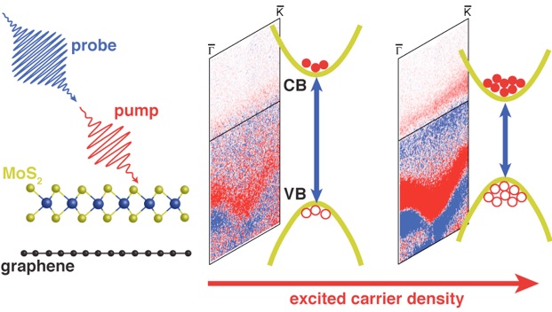
Ultrafast Band Structure Control of a Two-Dimensional Heterostructure, Søren Ulstrup, Antonija Grubišic Cabo, Jill A. Miwa, Jonathon M. Riley, Signe S. Grønborg, Jens C. Johannsen, Cephise Cacho, Oliver Alexander, Richard T. Chapman, Emma Springate, Marco Bianchi, Maciej Dendzik, Jeppe V. Lauritsen, Phil D. C. King, and Philip Hofmann, arxiv1606.03555
ACS Nano 10, 6315 (2016).
Quasi one-dimensional metallic band dispersion in the commensurate charge density wave of 1T-TaS2
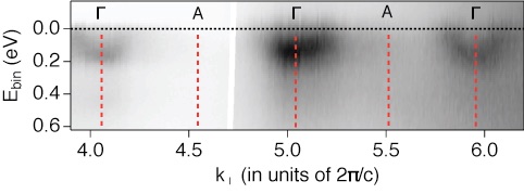
TaS2 in its 1T structural modification is a metallic transition metal dichalcogenide that has been studied for more than 40 years because of its many fascinating phase transitions at low temperatures. The new emerging phases are slightly different charge density waves of the electrons, along with a strong deformations of the lattice. The reason for these transitions are still subject to controversy, but both strong electron-lattice and strong electron-electron interactions are thought to be important. Until recently, 1T TaS2 was viewed as a stack of quasi independent TaS2 layers, held together by weak van der Waals forces, and it was tried to explain the charge density wave transitions in a simple two-dimensional picture. However, recent calculations have predicted a strong dispersion of an electronic band perpendicular to the TaS2 layers, i.e. electrons moving in that direction. In this work, we have been able to confirm this predicted dispersion experimentally, confirming that a quasi two-dimensional picture might not be sufficient to understand this complex material.
Quasi one-dimensional metallic band dispersion in the commensurate charge density
wave of 1T-TaS2, Arlette S. Ngankeu, Kevin Guilloy, Sanjoy K. Mahatha, Marco Bianchi, Charlotte E. Sanders, Kai Rossnagel, Jill Miwa and Philip Hofmann, arxiv1705.00455
Physical Review B 96, 195147 (2017).
Crystalline and electronic structure of single-layer TaS2
In its bulk form, TaS2 is a layered crystal similar to WS2 or MoS2, but with the important difference that TaS2 is a metal, not a semiconductor. It exists in two structural modifications and due to its metallic character, it is susceptible to different electronic instabilities such as charge density waves or superconductivity. In contrast to the semiconducting MoS2 or WS2, single layers of TaS2 cannot be peeled off by “the Scotch tape method” because the material is not air-stable. In this work, we report the first synthesis of single layer TaS2 and we investigate its electronic structure. It turns our, that the single layer is also metallic, but it does not undergo any instabilities down to the lowest temperatures we have investigated.
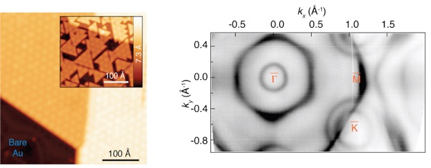
Crystalline and electronic structure of single-layer TaS2 Charlotte E. Sanders, Maciej Dendzik, Arlette S. Ngankeu, Andreas Eich, Albert Bruix, Marco Bianchi, Jill A. Miwa, Bjørk Hammer, Alexander A. Khajetoorians, Philip Hofmann, arxiv1606.05856
Physical Review B 94, 081404(R) (2016).
Electronic structure of single-layer MoS2
As in the case of graphene, many layered materials change their properties in subtle but important ways when thinned down to a single unit layer. Important examples of this are the transition metal dichalcogenites such as MoS2. While bulk MoS2 is a semiconductor with an indirect band gap, a single layer has a direct band gap. Moreover, the top of the valence band has been predicted to be split by the spin-orbit interaction. By growing high-quality epitaxial MoS2 layers on the (111) surface of gold and then inspecting these with angle-resolved photoemission spectroscopy on ASTRID2, we have been able to directly measure the band structure of single-layer MoS2 in unprecedented detail. In fact, the sample quality and resolution is so good that even the predicted spin-orbit splitting can be observed.
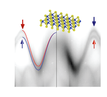
Jill A. Miwa, Søren Ulstrup, Signe G. Sørensen, Maciej Dendzik, Antonija Grubišic Cabo, Marco Bianchi, Jeppe Vang Lauritsen, Philip Hofmann, arxiv1410.0615, Physical Review Letters 114, 046802 (2015).
Spin-polarized bulk states in a bulk inversion-symmetric material
Spintronic is a new approach to electronic that uses the spin of the electrons rather than (or in addition to) their charge in order process or store information. A key ingredient of the technique is the ability to have materials with a spin-dependent electronic structure, i.e. electronic energy states that are different for different spin orientations. Spin-dependent energy splittings have recently been found for two-dimensional single layers of transition metal dichalcogenites such as MoS2 or WSe2. In these single layers such energy splittings are possible because of the low dimensionality that breaks the inversion symmetry present in the bulk. Indeed, the desired spin-splitting is forbidden for any bulk material with inversion symmetry. It therefore came as a big surpize when we recently found a strong spin polarization of the bulk bands in spin-polarized photoemission from bulk 2H-WSe2, a material that has inversion symmetry. This spin polarization for the top of the valence band near the corner of the Brillouin zone is illustrated in the figure below. They key to the puzzling result is that the heavy W atoms are locally not in an inversion symmetric environment and the spin-split states are strongly localized to W atoms in different layers and hence different local environments.

J. M Riley et al., arxiv1408.6778, Nature Physics, advance online publication, see also News and Views by John Schaibley and Xiaodong Xu, see also Material gives up its spin-splitting secrets, physicsworld.com, October 2014.
Slow decay of excited electrons in bilayer graphene
In the highlight below, we had demonstrated the possibility to use ultrafast high energy laser sources to access the dynamics of excited electrons in graphene. When performing a similar experiment for bilayer graphene, pronounced differences can be found: In the bilayer, the excited electrons remain far longer i the conduction band than in just a single layer of graphene, something that can be ascribed to the existence of a small band gap in this material. Interestingly, twisted domains in bilayer graphene are known to “short circuit” the band gap to some extend but our results nevertheless demonstrate the potential use of bilayer graphene for opto-electronic applications.
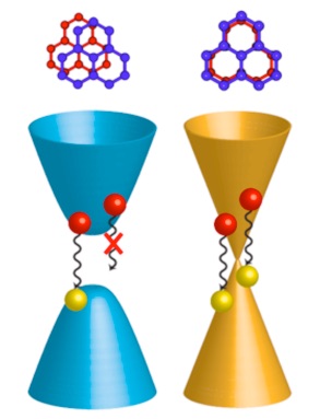
Søren Ulstrup, Jens Christian Johannsen et al., arxiv1403.0122, Physical Review Letters 112, 257401 (2014), see also Viewpoint in Physics 7, 68 (2014) by Luca Perfetti.
Watching optically excited electrons decay in graphene
Graphene has extraordinary optical properties. Despite of being only one atomic layer thick, it absorbs 2.3% of the light it is exposed to, and it does so over a very wide range of wavelengths. It has therefore been discussed if it could be possible to use graphene in light detecting or solar cell applications. For this to work, one needs to separate optically excited electron-hole pairs before they decay again. One can learn about the fate of the excited carriers in time-dependent pump-probe experiments, and when doing this with angle-resolved photoemission spectroscopy, one can even study the energy and k-resolved occupation of electrons and holes directly. This has long been an elusive goal because of the high photon energies needed to reach the Dirac cone which is placed at the K-point of graphene’s Brillouin zone. Using a high-energy laser source at the ARTEMIS laboratory of the National Laser Facility in the UK, such a direct view on the hot electron dynamics has now become possible.
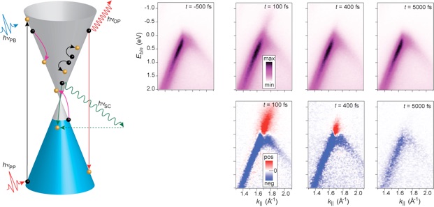
Jens Christian Johannsen, Søren Ulstrup et al., arxiv1304.2615, Physical Review Letters 111, 027403 (2013). Click on the image to view a movie of the full data set.
Probing the electronic structure of a buried two-dimensional electron gas
Confining electrons in (nearly) two dimensions can give rise to a so-called two-dimensional electron gas (2DEG). A 2DEG has fascinating physical properties, as seen in the quantum Hall effect, but it is also the key-ingredient of a field effect transistor and at the heart of modern electronics. A particularly clever way to create a 2DEG is by so-called delta-doping: a single sheet of dopant atoms is placed on the surface of silicon and then deeply buried under more silicon. The 2DEG then forms a metallic layer in the semiconductor and it can also be structured, by placing the doping atoms only at certain positions. Such buried 2DEGs have been widely studied by transport techniques but their band structure has never been measured directly. Using synchrotron radiation and a resonant enhancement of the emission from the 2DEG states, we have been able to directly probe the band structure of these interesting systems for the first time.
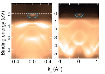
Jill A. Miwa et al., arxiv:1210.7113, Physical Review Letters 110, 136801 (2013).
Lifting epitaxial graphene from its substrate
High-quality graphene can be grown epitaxially on transition metal surfaces. In this process, there is a delicate balance between the crystalline quality and the graphene-surface interaction: For a strong interaction, one obtains single-crystalline graphene with only one rotational orientation but the electronic structure is also strongly influenced through the bonding to the metal. For a weak interaction, one obtains the desired electronic structure of nearly-free graphene but the metal structure does no longer dictate the orientation of the graphene flakes on the surface and several rotational domains are present. In this highlight, we show that graphene can be grown on a surface with a strong bonding to graphene but later lifted by oxygen intercalation, keeping the single crystalline graphene but weakening the interaction to obtain the electronic structure of quasi free-standing graphene. This approach opens the possibility to study the electronic structure of pristine graphene in a new way, but it may also pave the way to loosening the graphene from the metal substrate for an easier transfer.
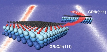
Rosanna Larciprete et al., ACS Nano 6, 9551 (2012)
Transfer-free electrical insulation of epitaxial graphene from its metal substrate
Graphene is one of the most promising materials for future electronic applications because of its very high carrier mobility, tolerance to high temperatures and inertness. Exploiting the electronic properties requires graphene to be placed on an insulating substrate, such as SiO2. This can be achieved by different routes, for example after exfoliation from graphite, after reduction of graphene oxide or after large-scale growth on metal films that are subsequently dissolved. Unfortunately, these methods result either in very small graphene flakes or in graphene of poor quality. A proven route to large-scale, single-crystal graphene is the epitaxial growth on transition metal surfaces but this has the disadvantage of a conductive substrate. In this work we demonstrate that such epitaxial graphene can be electrically decoupled from the metal it is grown on, by placing an insulating layer of SiO2 under the graphene. This can be achieved by the intercalation of silicon and oxygen and a step-wise reaction under the graphene layer. We demonstrate that the electrical decoupling is sufficient for transport to be dominated by the graphene sheet and not by the underlying metal. This route to graphene synthesis combines the advantages of high-quality growth with an insulating substrate, opening a novel route to device fabrication and fundamental studies of transport properties.

Silvano Lizzit et al., Nano Letters 12, 4503 (2012)
see also (arXiv:1208.2144)
Simultaneous quantization of bulk conduction and valence band states through adsorption of nonmagnetic impurities on Bi2Se3
In the highlight below (Large and tunable Rashba spin splitting….), we show that the clean surface of the topological insulator Bi2Se3, undergoes a time-dependent band bending that is strong enough to give rise to a substantial Rashba splitting in a two-dimensional electron gas (2DEG) near the surface. In this paper, we probe the origin of this band bending and show that it can be induced by exposing the surface to carbon monoxide. Most unusually, we do not only observe a quantization of the bulk conduction band states into 2DEGs but also a quantization of the valence band states into a ladder of quantum wells (shown in the figure below). We argue that such a simultaneous quantization of conduction band and valence band is only possible because of the special electronic structure of bulk Bi2Se3.
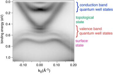
Marco Bianchi et al., Physical Review Letters, 107, 086802 (2011).
see also (arXiv:1104.4930v1), click on the image to view the quantum well formation as a movie.
Large and tunable Rahsba spin splitting of a two-dimensional electron gas near the surface of Bi2Se3
Electrostatic manipulation of the electron spin lies at the heart of the emergent field of spintronics. Currently, however, even the prototypical method for demonstrating such control via a Rashba spin-splitting of a two-dimensional electron gas (2DEG) is difficult to implement due to the small spin-orbit interaction in most semiconductors. In this paper, we report a Rashba splitting of a 2DEG in the topological insulator Bi2Se3, which is at least an order of magnitude larger than in other semiconductors. We further demonstrate that the spin-splitting can be controlled electrostatically, opening a route towards room-temperature operation of nanoscale spintronic devices. The figure below shows how the Rashba splitting of the the 2DEG evolves with time, from a 2DEG with no apparent splitting, to a strong splitting.
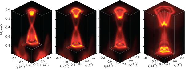
P. D. C. King et al., Physical Review Letters 107, 096802 (2011)
see also arXiv:1103.3220v1), click on the image to view the corresponding movie.
Coexistence of the topological state and a two-dimensional electron gas on the surface of the topological insulator Bi2Se3
Topological insulators are a recently discovered class of materials with fascinating properties: While the inside of the solid is insulating, fundamental symmetry considerations require the surfaces to be metallic. The metallic surface states show an unconventional spin texture, electron dynamics and stability. Recently, surfaces with only a single Dirac cone dispersion have received particular attention. These are predicted to play host to a number of novel physical phenomena such as Majorana fermions, magnetic monopoles and unconventional superconductivity. Such effects will mostly occur when the topological surface state lies in close proximity to a magnetic or electric field, a (superconducting) metal, or if the material is in a confined geometry. We show that a band bending near to the surface of the topological insulator Bi2Se3 gives rise to the formation of a two-dimensional electron gas (2DEG). The 2DEG, renowned from semiconductor surfaces and interfaces where it forms the basis of the integer and fractional quantum Hall effects, two-dimensional superconductivity, and a plethora of practical applications, coexists with the topological surface state in Bi2Se3. This leads to the unique situation where a topological and a non-topological, easily tunable and potentially superconducting, metallic state are confined to the same region of space. The figure below shows angle-resolved photoemission data revealing the 2DEG and the topological state.
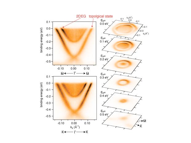
M. Bianchi et al., Nature Communications 1:128 (2010), DOI: 10.1038/ncomms1131
see also arXiv:1009.2879v1
Band gap narrowing near the surface of a semiconductor
The gap between valence band and conduction band of a semiconductor is one of its most fundamental properties. The presence and size of the gap is what makes a semiconductor device work. The function of many devices relies on band bending, an electrostatic effect in which the energy of both valence and conduction bands changes in the vicinity of a surface or an interface. In extreme cases, the bending can be so strong that new quantum well states appear at the interface, forming a two-dimensional electron gas. Here we show that the presence of such states, and the high electron density associated with it, can give rise to a considerable shrinkage of the band gap. This effect can be expected to be important for the engineering of actual semiconductor devices. The figure shows the spectrum of a quantum well state at a surface of CdO.
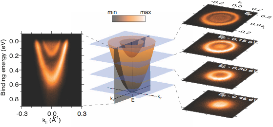
P.D. C. King et al., Phys. Rev. Lett. 104, 256803 (2010).
Band dispersion in the deep 1s core level of graphene
It is generally assumed that electrons in deep atomic core states are highly localised and do not participate in the bonding of molecules and solids. This implies well-defined core level binding energies and the absence of any splitting and band-like dispersion, a fact which is exploited in several powerful experimental techniques, such as x-ray photoemission spectroscopy. Violations of this assumption have only been found for a few small molecules in the gas phase such as acetylene or nitrogen with much stronger bonding and shorter bonding distances than present in solids. In this work we report the observation of a sizeable band-like dispersion of the C 1s core level in graphene, a single-layer honeycomb net of carbon atoms that is presently attracting considerable attention in the scientific community.
The dispersion is observed as an emission-angle dependent binding energy modulation (see sketch below) and it is shown that under appropriate conditions only the bonding or anti-bonding states can be observed.

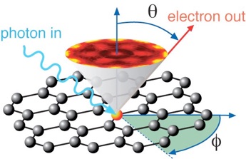
S.Lizzit et al. Nature Physics s 6, 345 (2010).
Bandgap opening in graphene induced by patterned hydrogen adsorption
Graphene, a single layer of graphite, has recently attracted considerable attention owing to its remarkable electronic and structural properties and its possible applications in many
emerging areas such as graphene-based electronic devices. The charge carriers in graphene behave like massless Dirac fermions, and graphene shows ballistic charge transport, turning it into an ideal material for circuit fabrication. However, graphene lacks a bandgap around the Fermi level, which is the defining concept for semiconductor materials and essential for controlling the conductivity by electronic means. Theory predicts that a tunable bandgap may be engineered by periodic modulations of the graphene lattice but experimental evidence for this is so far lacking. In this paper, we demonstrate the existence of a bandgap opening in graphene, induced by the patterned adsorption of atomic hydrogen onto the moiré superlattice positions of graphene grown on an Ir(111) substrate. The figure illustrates the structure and electronic structure of the clean and hydrogen-covered graphene.
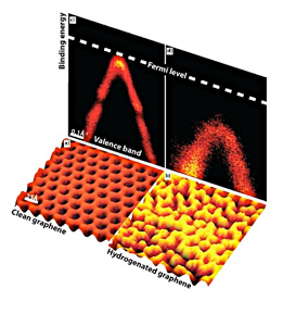
R. Balog et al. Nature Materials 9, 315 (2010).
Direct measurement of conductance through a self-assembled molecular layer
The self-assembly of organic molecules on surfaces is a promising approach for the development of nanoelectronic devices. While a variety of strategies has been employed to establish stable links between molecules, little is known about the electrical conductance of these links. Extended electronic states, a prerequisite for good conductance, have been observed for molecules adsorbed on metal surfaces. However, direct conductance measurements through a single layer of molecules are only possible if the molecules are adsorbed on a poorly conducting substrate. Here we use a nanoscale four-point probe to measure the conductivity of a self-assembled layer of cobalt phthalocyanine (CoPc) on a Ag-terminated Si surface as a function of thickness. For low thicknesses, the CoPc molecules lie flat on the substrate and their main effect is to reduce the conductivity of the substrate. At higher thicknesses, the CoPc molecules stand up to form stacks and begin to conduct. These results connect the electronic structure and orientation of molecular monolayer and few-layer systems to their transport properties, and should aid in the rational design of future devices.
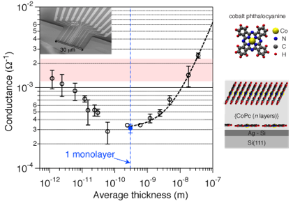
F.Song et al. Nature Nanotechnology 4, 373 (2009).
Electrons with opposite spins move in opposite directions
In one dimension, there are only two ways to move: left or right. This leads to some peculiar properties for one-dimensional systems on the atomic scale. In our paper we present a one-dimensional conductor forming on a bismuth surface, which effectively separates the electrons going through it according to their spin, a kind of rotation around the electron’s axis. It turns out that electrons going to the left have exactly the opposite spin as electrons going to the right. Such a situation could have useful applications in the field of spintronics, a novel type of electronics which is based on the electron’s spin rather than its charge and which could lead to more effective computers or even quantum computing. The state is in several ways similar to so-called edge states appearing in the recently discovered quantum spin Hall effect but instead of being found for a sandwich structure of semiconductors at very low temperatures, it is found on a simple, clean surface, is truly one-dimensional and, most remarkably, even exists at room temperature.
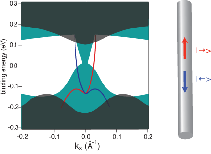
J.W. Wells et. al., Phys. Rev. Lett. 102, 096802 (2009)
The discovery of the acoustic surface plasmon
Surface plasmon is the name for an electron density wave which propagates on the surface of a conductor, very similar to water waves on the surface of the sea. These electron waves have recently been studied intensely due to the vast range of possible technical applications, especially in nano-optics, microscopy, light generation and optical data processing.
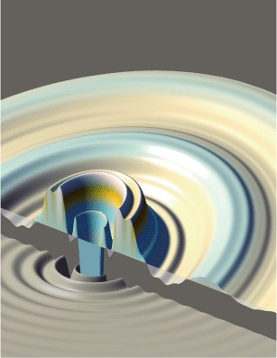
Unlike water waves, a lot of energy is needed to kick off a surface plasmon wave. Surface plasmons have therefore been thought to be unimportant in many processes, e.g. chemical reactions, where not enough energy is available to create them. Many scientists working in the field were therefore surprised by a theoretical discovery made by scientists at the Donostia International Physics Centre in Spain who predicted the existence of a new kind of surface plasmon, the so-called acoustic surface plasmon, which could be excited with very small energies. The theoretical prediction and the fascination of this completely new phenomenon sparked an intense experimental effort to proof the existence of the acoustic surface plasmon, an endeavour which has now finally succeeded on the (0001) surface of the metal beryllium.
The figure shows a visualisation of the acoustic surface plasmon. The lower part shows a static electronic wave induced by a charge close to the surface. The upper part shows what happens when the charge close to the surface is not fixed but moved: the novel type of propagating electron wave is generated and superimposed on the static wave.
As with many new discoveries, it is difficult to appraise their possible impact. The key element of the new plasmon is its acoustic character, i.e. that plasmon waves can be excited with very small energies (like water waves), allowing them to participate in many dynamical processes at surfaces such as chemical reactions. Another interesting possible application lies in the interaction of the new plasmon with light, which could be confined to nano-scale areas on the surface of a conductor.
B.Diaconescu et al., Nature 448, 57 (2007).
Disentangling surface, bulk and space-charge layer conductivity: Si(111)(7×7)
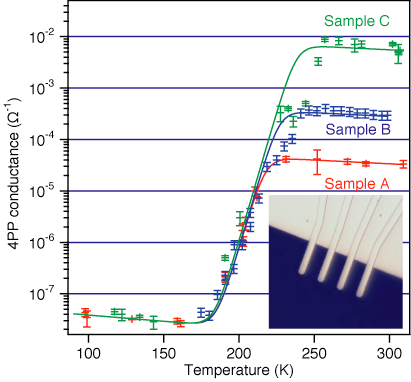
Understanding the conductance of a material is one of the most fundamental tasks in solid state physics. Precise conductance measurements are usually carried out using a (macroscopic) four point probe. Recently, microscopic versions of four point probes have been developed which allow surface-sensitive conductance measurements and, in principle, conductance measurments on nano-structures. Using such a microscopic four point probe, we have studied the Si(111)(7×7) surface, the electronic character of which has been disputed for a long time. Its temperature dependent conductivity was measured with a microscopic four point probe between room temperature and 100 K. At room temperature the measured conductance corresponds to that expected from the bulk doping level. However, as the temperatures is lowered below approximately 200 K, the conductance decreases by several orders of magnitude in a small temperature range and it saturates at low temperatures, irrespective of bulk doping. This abrupt transition is interpreted as the switching from bulk to surface conduction, an interpretation which is supported by a numerical model for the measured four point probe conductance. The value of the surface conductance is considerably lower than that of a good metal.
The figure below shows the temperature-dependent conductance of Si(111)(7×7) for samples with a different bulk doping as measured with a microscopic four point probe. At high temperature, the measurement is bulk sensitive and the conductance depends on the bulk doping. At low temperatures, the conductance is solely due to the surface and does not depend on the bulk doping. The inset shows an image of a typical microscopic four point probe as viewed through an optical microscope.
J.Wells et al. Phys. Rev. Lett., 97, 206803 (2006).
The role of the spin in quasiparticle interference
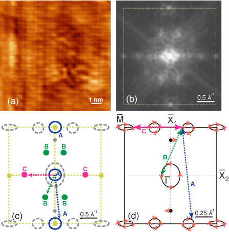
Quasiparticle interference is of fundamental importance to screening in metals. On surfaces and on high-temperature superconductors, interference patterns observed by scanning tunnelling microscopy (STM) can also be used to study the local electronic structure. Here we show that the spin of the quasiparticles can have a profound effect on the interference patterns. On Bi(110), a system with non spin-degenerate surface state bands, the patterns are not simply related to the dispersion of the electronic states. In fact, the features which are expected on grounds of the surface state and Fermi contour topology are absent and the only observable interference patterns can be assigned to spin-conserving scattering events.
The figure below shows (a) the quasiparticle interference pattern observed on Bi(110) together with (b) a Fourier transform in order to extract the main periodicities. (c) and (d) explain the main scattering events which lead to the structures in (b), taking into account the spin of the quasiparticles. evident.
J.I. Pascual et al., Phys. Rev. Lett. 93, 196802 (2004).
Strong spin-orbit splitting on bismuth surfaces
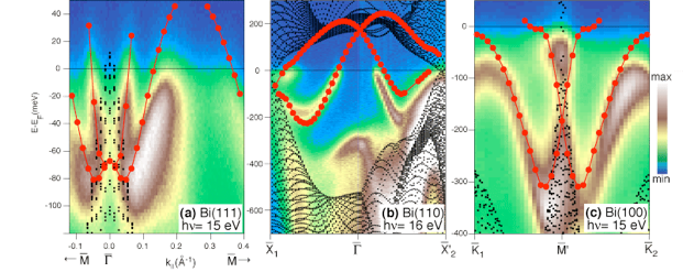
Using first-principles calculations and angle-resolved photoemission, we have recently shown that the spin-orbit interaction leads to a strong splitting of the surface state bands on low-index surfaces of Bi. The dispersion of the states and the corresponding Fermi surfaces are profoundly modified in the whole surface Brillouin zone. This has implications with respect to a proposed surface charge density wave on Bi(111) as well as to the surface screening, surface spin-density waves, electron (hole) dynamics in surface states, and to possible applications to the spintronics.
The figure shows the calculated surface state dispersion (red markers) together with the measured dispersion for some selected Bi surfaces (photoemission intensity as colour map). The agreement between experiment and calculation is excellent, but only if the spin-orbit interaction is taken into account.
Yu. M. Koroteev et al. Phys. Rev. Lett. 93, 046403 (2004).
